Microfabrication Laboratory (Cleanroom)
Introduction
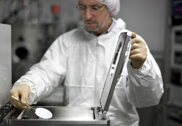
The microfabrication laboratory, a cleanroom with air lock and independent air conditioning and filtering system, is a cornerstone to the institute's infrastructure. The lab is run by the detector group's cleanroom personnel and is specialised in the fabrication of superconducting devices for our radioastronomy application. It is fully equipped with the thin-film and microstructuring capabilities needed to fabricate superconducting detector devices and silicon micromechanical structures, very similar to what is used in the semiconductor industry.
The cleanroom lab space consists of five rooms with four of them being connected with common air lock for entry:
- deposition lab: tools for deposition of thin films
- etcher lab: reactive-ion etcher for structuring of thin films
- litho lab 1: optical lithography with mask aligner, inspection microscope and wet chemical processing, yellow lighting
- litho lab 2: wet chemical processing and inspection microscope, yellow lighting
- ebeam lab: e-beam lithography tool and device mounting facilities
In addition, there are auxilliary rooms for dicing and lapping of wafers (i.e. "dirty processes") as well as storage of consumables and spares.
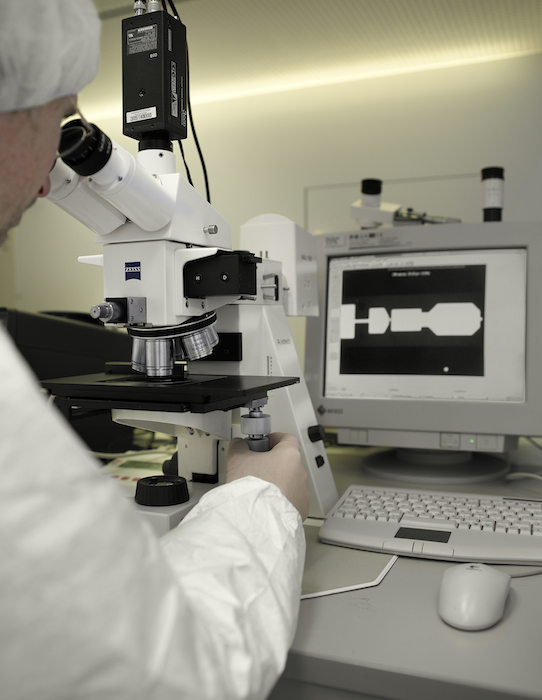
The lab was founded in 1989 and the first 230 GHz SIS junctions were already successfully fabricated in early 1990. The laboratory features a suite of lithographic tools to define device structures down to the nanometer range by means of electron-beam lithography as well as deposition equipment for the materials required for our circuits, e.g. superconductors, normal metals and dielectrics and an inductively coupled plasma (ICP) etcher for structuring of thin film and MEMS structures. These tools are completed by two lithography rooms with wet benches for liquid chemistry processing, resist spinners and hot plates and yellow lighting for handling of photosensitive materials. For quick inspection several high high power (magnifications up to 1000x, with differential interference contrast) optical microscopes from Zeiss are available.
With the support of an engineer and a technician and under supervision and assistence by senior scientists, many PhD students have earned their doctoral degree with fabrication of devices as part of their thesis work.
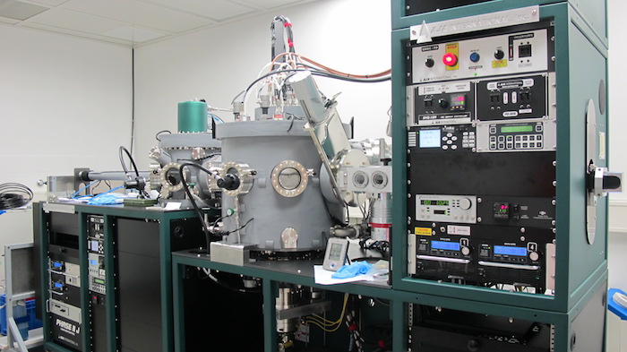
ICP Plasma Etcher (Oxford Instruments Plasmalab System 100)
The Oxford Instruments Deep Reactive Ion Etcher (DRIE) uses independent inductively-coupled and RIE plasma sources for etching (removing) of our thin film materials. This state-of-the-art tool features cryogenic and Bosch Silicon etching capabilites that are heavily used for structuring of ultra-thin substrates with SOI technology and for silicon micromachining (MEMS) of e.g. optical components such as the AR structured Si vacuum windows used in our THz receivers. The MEMS capabilities are crucial for the waveguide devices we develop and allow the micrometer precise definition of arbitrarily shaped (by means of photolithographic processes) Si membranes. For the so-called Bosch process the etcher features a dual-beam interferometer for precise in-situ measurement and online end-point detection of etch depth. In single beam mode reflectometry is used for determination of end-point, e.g. during etch of SIS junctions or HEB microbridges.
Electron Beam Lithography System (Raith PIONEER)
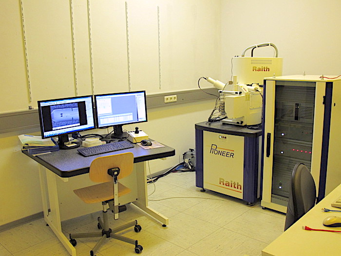
Our state-of-the-art Raith PIONEER electron beam lithography system, in use since September 2013 and equipped with a field emission source and a laser interferometer stage, is used for fabricating devices with dimensions reproducible better than 50 nm. With the laser interferometer high resolution stage writing fields, e.g. 100 µm x 100 µm, can be stitched with better than 50 nm repeatability. Compared to our old home-grown e-beam system, which was decommissioned ever since this tool went online, the vastly expanded capabilities of this e-beam tool allow us stitch together the RF circuits of the THz mixers, e.g. for the 4.7 THz HEB mixer, under fully automated software control. Only its significantly improved imaging (writing) optics allowed a precise control of the lithography processes required for fabrication of our 4.7 THz HEB mixers. Its capability is more than sufficient for future higher frequency work.
The much higher lithographic resolution achievable of this system, when compared to optical lithography (see below), comes with the disadvantage of longer processing times. Already in the design stage of a new detector circuit we take this into account and with typical result of employing a mix and match approach using e-beam for the critical structures (THz RF circuit, SIS junction, tuning circuit, HEB microbrigde and contacts) and the much faster mask aligner lithography for everything else.
Optical lithography (Karl Süss MJB3)
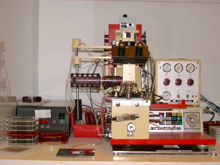
One Karl Süss MJB3 contact mask aligner is used for photolithographic definition of larger, wafer-scale structures such as wiring to each device. This tool has been around since 1989 and is the workhorse for quick lithographic processing not only of device structures but also IF circuits etc.. Due to the UV300 option (Hg light source, 320 nm line) the mask aligner can reliably define structures down to 0.8 µm line width. Optical photolithography is much faster than the more powerful e-beam lithography.
During circuit design a trade-off always has to be made between the two lithography options, e.g. resolution vs. speed. Typically our circuits are defined by a mix and match technique, i.e. using e-beam lithography for the critical areas on the wafer and optical lithography for everything else.
Deposition Tools
Sputtering
We currently operate two sputtering tools for deposition of the materials required for our detector development incl. superconductors (Nb, NbTiN, NbN), normal metals (Au, Al, Ti) and SIS tunnel barriers (Al2O3, AlN). Both feature multiple sputter guns with DC or RF capability, plasma cathodes and are load-locked. On both systems the sputter chambers are pumped by a large cryo pump in order to enable high process gas flow rates.
The new AJA Int. UHV sputtering tool (commissioned in 2017) is a load-locked multi-deposition system and is currently becoming our main deposition tool for future SIS, HEB and MKID device development and for materials development using a co-sputtering feature. The system features a sputter chamber with five 4" and, additionally, two 1.5" confocal sputter sources, and a second chamber for nitridation with an ICP source. The tool includes several substrate station options incl. 1000°C heating as well as RF for substrate biasing and rotation. Due to its larger diameter sputter guns this system will allow processing of 4" wafers with good thin film uniformities, which is required for future larger scale planar circuits such as MKID arrays and integrated 2SB/balanced SIS mixer devices. The system is fully bakeable with base vacuum in the 1E-10 mbar range.
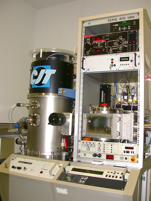
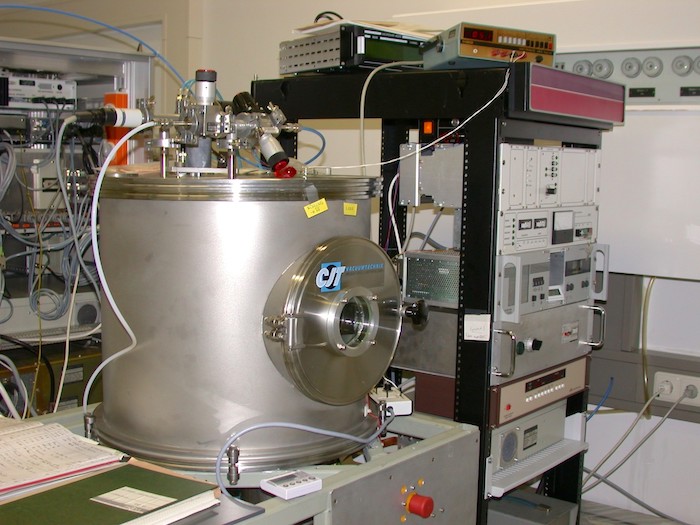
The CJT is our trusty old trilayer system for 2" wafers in operation since 1989 with base vacuum in the mid 1E-9 mbar range. It is mainly used for the standard Nb/AlOx/Nb trilayer processes as well as the Au normal metal layers for our THz circuits and HEB contact pads.
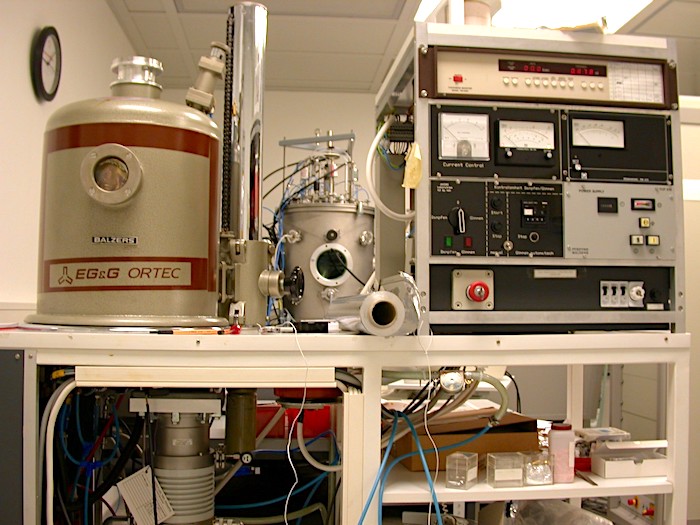
An 4 3" gun system from 4-tec (installed 1999) was decommissioned in 2017 and was the basis of our past NbN HEB layer and AlN SIS tunnel junction development, using a 1000°C heater station and in-situ ICP source. Its capabilities are being fully replaced by the much more powerful AJA tool.
For deposition of dielectric materials (SiO2, Si, SiN) we operate a separate system with 3" RF sputter gun. The SiO2 is mainly used as dielectric for our planar circuits. Equipped with a cryo pump the base vacuum is in the 1E-7 mbar range.
Evaporators
One self-made bell-type thermal evaporator is used for deposition of various materials, incl. SiO for circuit dielectric as well as the normal metals Au and Cu. It features a plasma clean capability with base vacuum in the 1E-6 mbar range. The RF sputterer mentioned above also features an e-beam evaporator source for material development.
Lithography Labs
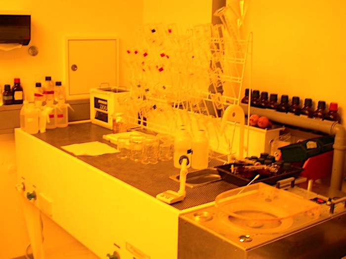
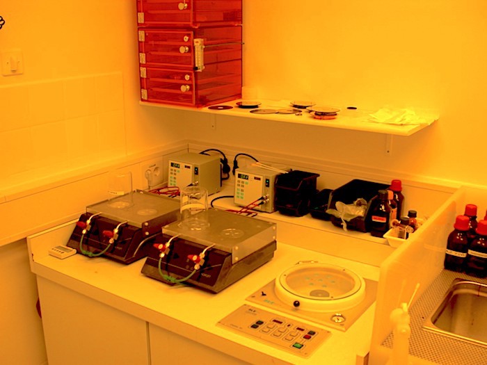
Our cleanroom is equipped with two lithography labs, litho 1 and 2, that use yellow lighting in order to allow processing with photosensitive materials such as photoresist. Litho 1 is equipped with the mask aligner as well as a process oven for baking of e.g. thick photoresists. Both labs feature high resolution optical microscopes (Zeiss Axioscope, 1000x magnification) with differential interference contrast and imaging systems for metrology. Both labs feature wet benches with their own fume extraction for processing with liquid chemicals such as organic solvents, photoresist related chemicals or acids. For resist processing each lab is equipped with a spinner and two hot plates with precise temperature control (+/- 0.1°C).
Device mounting and contacting
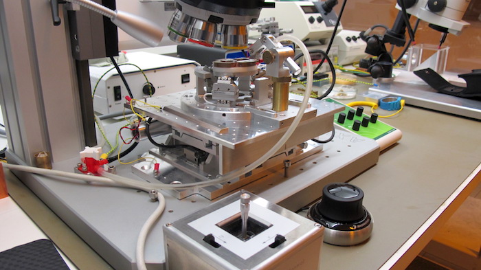
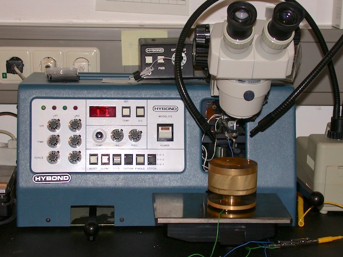
For mounting of our detector devices with the micrometer precision that THz waveguide circuits require we have developed our specialised setup based on a hexapod stage (SmarPod™) with 6-degrees of freedom. A single device is held by a vacuum tweezer and carefully aligned with the waveguide structures using this a remote control unit. Naturally a high power microscope is required for this handling. For reproducible mounting procedures of many devices, i.e. for the focal plane arrays that we populate, this nano-robotic tool has proven to be invaluable.
A wirebonder (Hybond 522) is used for contacting the devices and circuits. Tradionally wedge bonded 25 µm diameter aluminium or gold wires are used, currently mostly only used for connecting IF circuits.The membrane type mixer devices that we developed in the recent years to not need wires any more for contacting, as we provide the devices with beamleads during microfabrication. The beamleads not only suspend and palce the devices in the waveguide environment but also serve as DC and RF contact. For this we swap out the usual wedge with a tab bond tool.
Additional tools
Wafer processing
For "dirty processes" we have an auxiliary room outside of the cleanroom area, which holds to dicing saw and lapping machine. A wafer dicing machine (Tempress) is used to cut out devices of eg. 1800 µm x 50 µm x 30 µm from the quartz or silicon wafer on which the devices are fabricated. Before we had the DRIE capability only rectangular shaped devices therefore could be cut. For all membrane-beamlead type devices that run through the DRIE process we do not need the dicing saw anymore and only use it to dice section from wafers for DC characterisation of several devices a time.
A crystal polishing machine (Logitech PM4) available for precision lapping of substrates or wafers down to to about 30 µm thickness with micrometer precision.
Thin film profilometer
A thin film profilometer (Tencor Alphastep) is available in order to measure film thickness down to 5 nm. It is used for quick process control of deposited thin films and e.g. for establishing current sputter rates.
Chemical planarization process
In the cleanroom have a dedicated chemical-mechanical polishing (CMP) setup for planarisation of dielectric layers e.g. for SiO2. Similar to what the industry required CMP for their multi-layer circuits we use this CMP setup in the past for planarisation and contacting structures that are isolated in a dielectric e.g. the SIS junction top electrode. CMP allows very small and high quality junction areas to be defined.
Electroplating Setup
We use a simple electroplating setup for growing of our thick (2-3 µm) beamlead structures that all new heterodyne devices are based on. The setup is placed onto one of the wet benches when required.