Current HEB mixer research

Superconducting 1.9 THz Integrated Balanced HEB Mixers
Balanced mixers are good candidates for building focal plane array receivers, because they separate the RF and local oscillator (LO) inputs from each other. So there is no need for an external optical diplexer / beam splitter. In addition the near carrier noise of the LO on the mixer output is suppressed.
For e.g. the upGREAT array receiver the effectively used LO power is about 10 % of the available power while 90 % of it is transmitted through the beamsplitter and dumped. Therefore, balanced HEB mixers at 1.9 THz are developed. Of course this type of mixer configuration contains two HEB mixers, which needs double the LO power. However due to the no longer necessary beamsplitter about 40 % more of the LO power is used compared to the single ended mixer configuration.
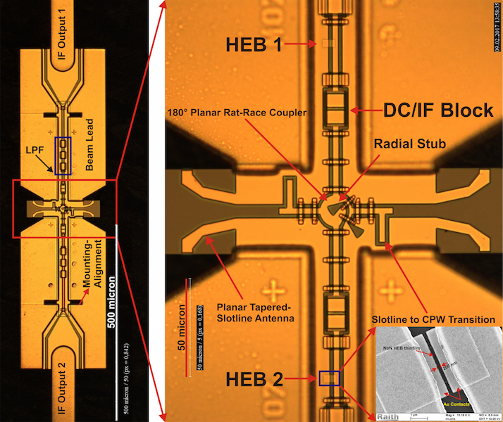
Optical microscope image of the fabricated integrated 1.9 THz balanced HEB (M07 device number) with two HEBs and two low pass filters (LPF), one per each arm. There is also a zoom on the planar ring coupler, planar antennas, slotline to coplanar transitions, two HEB bridges (additional SEM image of one of the bridges) and two DC/IF blocks.
The planar balanced mixer circuit, fabricated in 200 nm thick Au, is designed on a 3 μm high resistivity silicon membrane to avoid any possible waveguide modes. Heart of the circuit is a 180° planar ring coupler to equally divide two incoming signals by 180° and 0° phase difference respectively. The 180° coupler has the advantage of higher isolation between LO and sky signal in comparison to 90° hybrid. Ambitiously, the RF-part of this 1.9 THz mixer circuit is fully integrated on one thin substrate, and we have variations with two or four equal HEB bridges on one chip. The chip is registered on the waveguide (split-) block and contacted with beamleads.
An important requirement is to obtain the about 4.5 nm thick NbN HEB bridges on one chip with similar DC current at critical voltages (Ic) and critical temperatures (Tc). This is achieved by the close proximity of the bridges on the wafer and by accurate high resolution E-beam lithography definition of the lateral dimensions of the bridges. A first batch of devices with a Tc about 7.8 K was fabricated.
The split waveguide blocks (waveguide dimensions: 100 μm x 50 μm) have been fabricated in house from CuTe. The transmission of machined balanced waveguide blocks, without a mixer device, is characterized by our THz time domain spectrometer (TTDS) and compared to the transmission of 2 (upGREAT LFA-) horns back to back.
For the mixer devices, up to now, we could show a fairly equal power division (see Fig.) of incoming LO-power over the 2 mixers from both input ports. The phase relation of the input ports is also proven in heterodyne mode, using a narrow band source as signal. We bias the 2 HEBs with the same or an opposite polarity DC-voltage and read the output power at the sigma or delta port of an external 0.7 – 2.2 GHz 180° IF hybrid coupler with a spectrum analyzer. We show that upon changing the bias polarity of one mixer, the signal is suppressed completely.
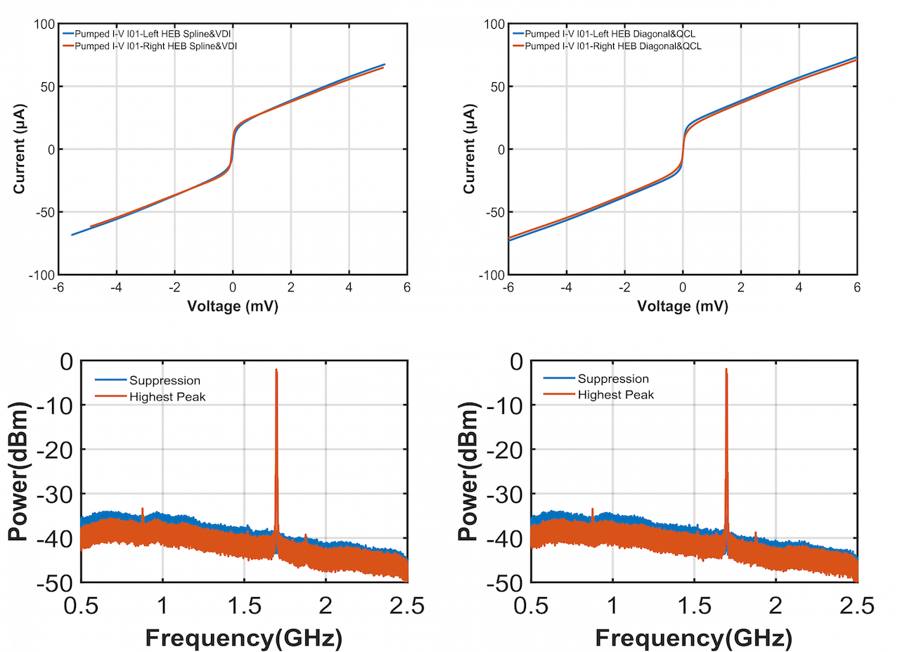
Measured IV-curve of left and right HEBs of the integrated 1.9 THz balanced HEB mixer device I01 when pumping the device with, Top-Left: VDI source at the signal port, Top-Right: QCL LO at the diagonal horn port. IF output spectrum of the balanced mixer applying attenuated VDI LO source at the signal side and full pump QCL at the LO port (diagonal horn side, Bottom-Left: Suppression and highest peak reading at the Sigma port when DC biasing HEB bridges same and opposite polarities, respectively, Bottom-Right: suppression and highest peak reading at the Delta port when DC biasing HEB bridges opposite and same polarities, respectively.
Development of 10.7 THz HEB mixer

Fig 2: Cross section through a setup with a hemispherical lens. A point source placed at coordinate (0,0) emits radiation which is collected by a screen (blue) placed at x=20 in parallel to the z-axis. The rays (dashed lines) starting from the point source are partly refracted by the silicon lens. All rays which suffer total reflection are not plotted and lead to two empty angular areas which are symmetrically arranged around the z-axis. The image has been created with our new developed software program.
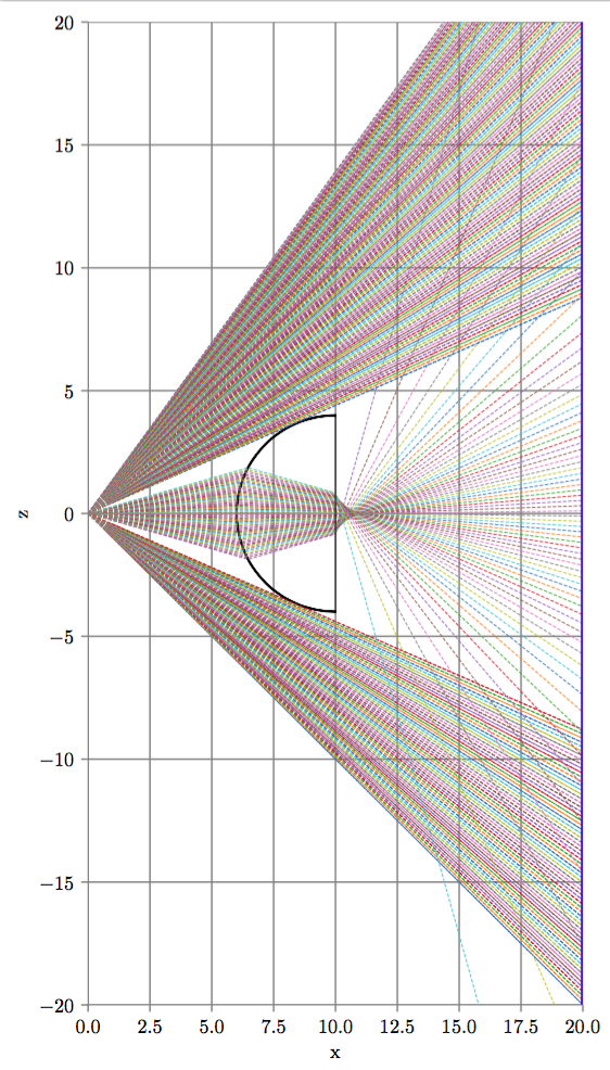
Fig 1: Schematic view of an open design mixer: The THz radiation (red) impinges the lens surface and is focused onto the antenna structure of the planar antenna system chip.
The para-H2 molecule has a lowest energy transition J=2→0 at 10.623 THz (28.22 μm). The direct detection of it's weak emission feature (small Einstein coefficients) of electric quadrupole transitions demands high resolution which only a heterodyne system supplies. The highest sensitivity heterodyn mixers at this frequency are realized with HEB mixer devices . Due to the approx. factor 2 higher frequency as compared to our current highest frequency mixer at 4.7 THz, which was on the limit that current technology and tolerances would allow, we decided to implement different technologies for the mixer at 10.7 THz.
Our current work concentrates on a mixer using a planar antenna rather than a waveguide with horn to couple to free space. The NbN HEB as the mixing device is integrated with the Au antenna on a high resistivity silicon substrate that is mounted on a silicon lens. Besides the small dimensions of the antenna and HF-filter structures which are decreased by roughly a factor about 2.5 due to the high dielectric constant of silicon, an additional challenge is given by the radiation losses of the HF transmission lines. For such increasing frequencies the standard equations for calculating the characteristics of the transmission lines becomes inaccurate and need to be carefully evaluated to avoid unwanted frequency shifts as reported in [1].
As we are limited in computational resources, the commercial software CST programm studio suite which we use for our HF circuit calculations cannot be applied to the complete design, due to the in comparison to the wavelength of operation λ0 large volume of the lens. It needs to be discretized into typical cell sizes of λ0/10 and smaller for numerical solver which exceeds our available memory and computationally time. To calculate the influence of the lens on the beam pattern of the antenna structure we have developed a software which uses backward ray tracing with a classical spectral domain approach method as described in [2]. Besides lenses, ellipsoids and other standard optical elements the modularly structured software can be extended by any analytically definable geometrical bodies. The software allows for highly efficient parallelization.
Materials
There is considerably room for improvement in the performance characteristics of our HEB mixers. The measured mixer noise performance is still 5 to 10 times the theoretical quantum limit for heterodyne detection. A deeper understanding of the fundamental noise processes that are relevant for mixing and detection is not available and therefore device engineering is hindered (see section on device physics below). Measured IF noise bandwidths are only 4 GHz for a typical NbN on Si substrate device and impacts overall receiver efficiency as it limits the instantaneous detection bandwidth of the system. The measured values are lower than the expected for bulk materials and point to reduced transparency of the microbridge to substrate interface.
The development of new material systems are generally required to further improve device performance. Our focus will be on the HEB microbridge layer itself and the phonon-transparency of the interface between microbridge and substrate:
- Newly available superconducting materials, in particular MgB2 thin films with significantly higher Tc >30 K (bulk 40 K) vs. 10 K for NbN, have been developed by other groups for HEB mixer application.The higher Tc helps twofold: Firstly, the electron-phonon interaction time taue-ph scales ~ Tc-3. Secondly, the phonon escape time inversely scales with the thickness of the microbridge layer tauph-esc ~ d, and developing microbridge material that stays superconducting for nanometer thin films is mandatory. MgB2 thin films show great promise to advance HEB mixer performance significantly due to IF noise bandwidths above 10 GHz already being demonstrated, see e.g. Novoselov et al., IEEE Trans. on THz Sci. and Techn., 7(6):704–710, Nov 2017. We plan to invest in MgB2materials development for our HEB devices. A dedicated thin films materials development is required, as the materials processing needs to be locally integrated into our device fabrication for efficient optimization. For this a specialized CVD deposition tool will need to be developed.
- Improving the phonon acoustic mismatch between the microbridge and substrate, which arises from the the materials dependent phonon velocities, by either selection a more suitable materials combination and/or introducing a buffer layer at the interface with certain matching characteristics. Currently HEB mixers using NbN on GaN substrates show a significant improvement in measured IF noise bandwidths. 7 GHz have been very recently demonstrated by Krause et al., IEEE Trans. on THz Sci. and Techn., 8(3):365–371, May 2018. Compared to current NbN on Si technology this leads to nearly a two-fold improvement in instantaneous bandwidth of a receiver. We believe it is straight-forward to modify our existing NbN thin film process to GaN substrates, and that should be pursued.
Device Physics
Gaining a complete physical understanding of the complex scattering mechanisms in a DC + RF driven superconducting material thin film microbridge operated at its transition edge is a truly "Herculean task" and will need a lot of effort. Understanding the source of mixer noise and other performance characteristics in a HEB microbridge is beneficial for optimization of the device materials, geometry and layer schemes. Without a qualitative and, ideally, quantitative description we (and everyone else) currently need to base HEB device development on various empirical or semi-empirical approaches. Currently the noise performance of these devices still is several times above the quantum limit less predicted RF circuit losses. Therefore there is a strong research opportunity is on hand, to employ a bottom-up approach and look at various scattering processes in these microbridges under specific operation conditions, therewith working towards the bigger picture, ultimately physics engineering the devices to maximum performance
Acknowledgements
Balanced HEB mixer and 10.7 THz HEB mixer development are carried out within the Collaborative Research Centre 956, sub-project D3, funded by the Deutsche Forschungsgemeinschaft (DFG).
References:
[1] Focardi, Paolo, William R. McGrath, and Andrea Neto. "Design guidelines for terahertz mixers and detectors." IEEE Transactions on microwave theory and techniques 53.5 (2005): 1653-1661
[2] Ehtezazi, I. A., and C. Letrou. "A spectral domain ray tracing method for quasi-optical devices modelling." Antennas and Propagation Society International Symposium, 1998. IEEE. Vol. 2. IEEE, 1998.