Waveguide coupled Microwave Kinetic Inductance Detector

Microwave Kinetic Inductance Detectors (MKID) are superconducting power detectors suitable for a wide frequency range from about 50 GHz up to the X-ray frequencies.The kinetic inductance of a superconducting piece of material is changed by an increase of the number quasi particles caused by the detected photons. The change in kinetic inductance is measured by placing the kinetic inductor in a narrow band ( <1MHz) resonant circuit. If the kinetic inductance changes, both the frequency and the amplitude of the resonance change. This is resonance is monitored by a read-out signal that is weakly coupled to the MKID circuit and amplified with a cryogenic low-noise amplifier . Resonacesed are typically chosen to be in the frequency range of 0.1-10 GHz. It is possible to read out many MKID's with a slightly different resonance frequency with a moderate bandwidth cryo-LNA. This frequency multiplexing of MKID's makes it possible to build cameras or spectrometers with many thousands of pixels.
A 350 GHz Waveguide Coupled KID design

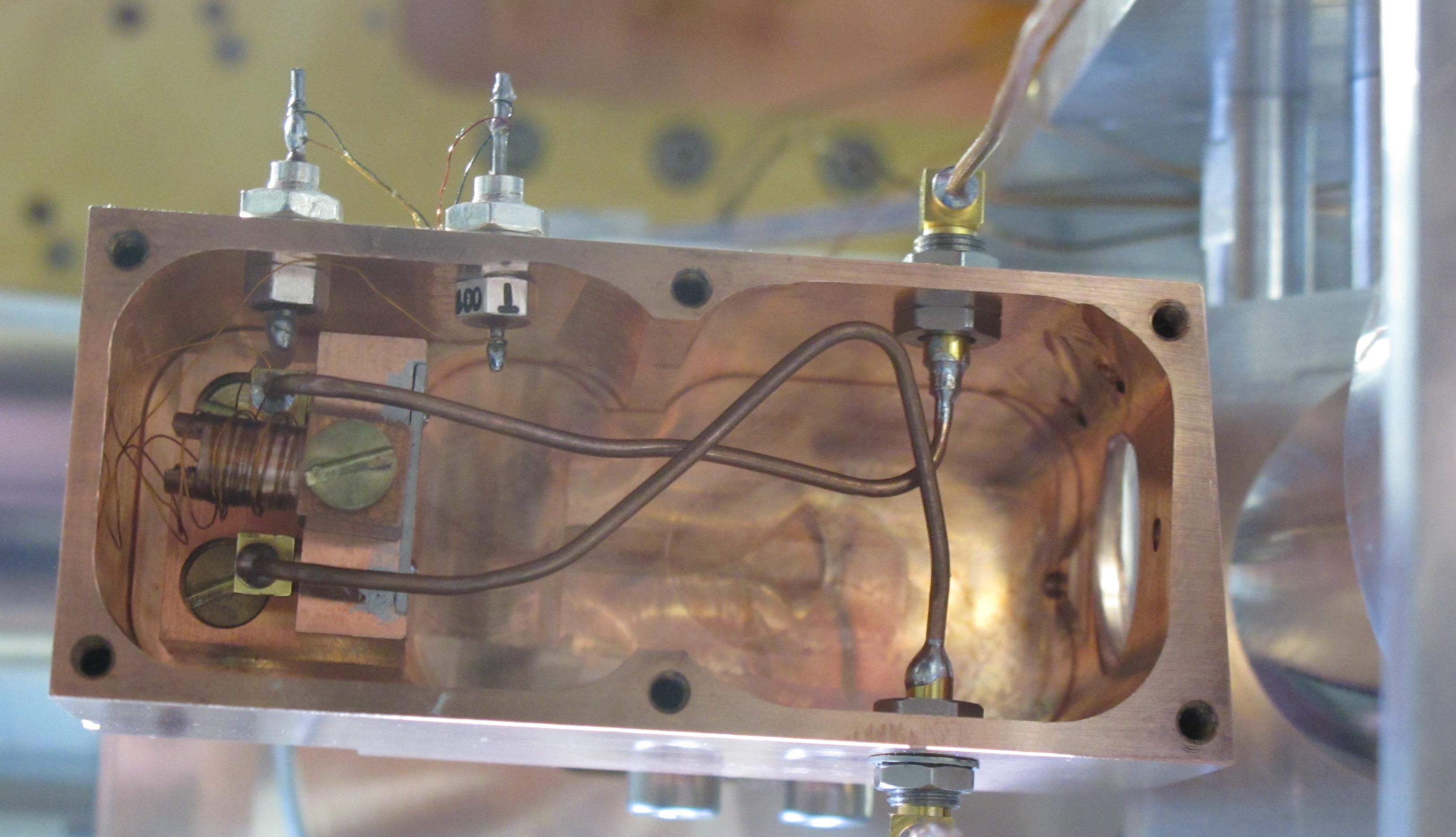
We investigate the sensitivity and noise of Microwave Kinetic Inductance Detector (MKID) devices that are coupled to a waveguide utilizing a proven waveguide probe antenna. This 350 GHz design originates from a SIS mixer and guarantees good radiation coupling to the detector, and facilitates analysis of the MKID device performance itself.
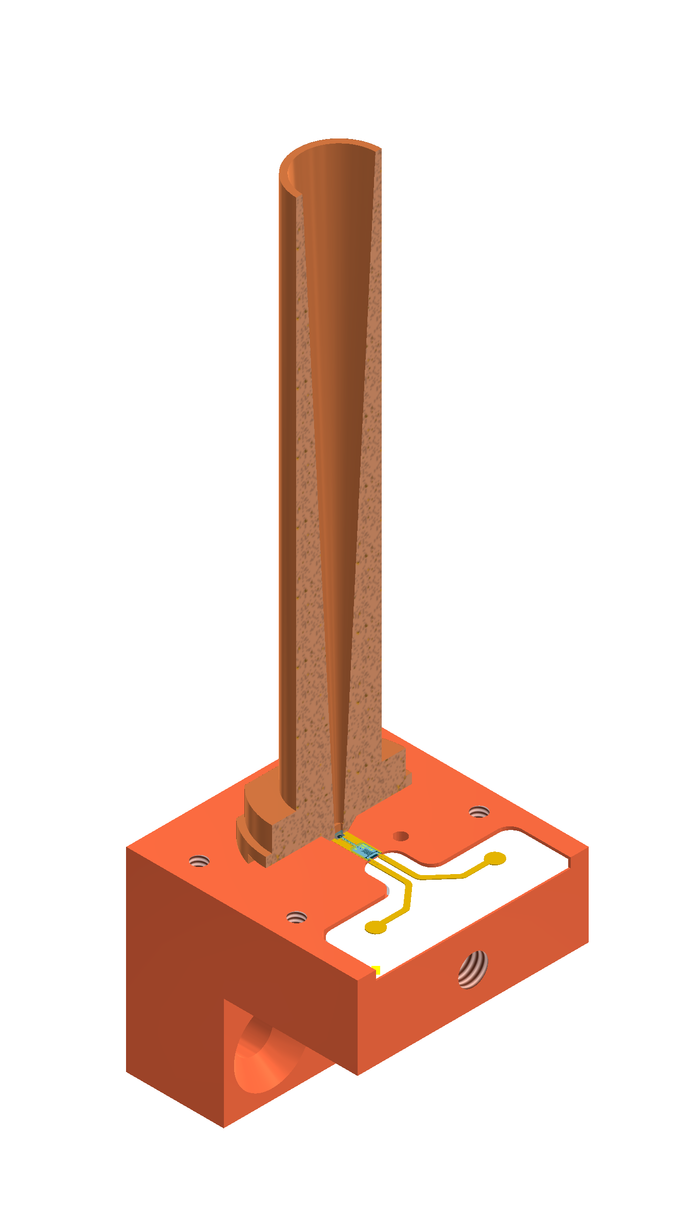
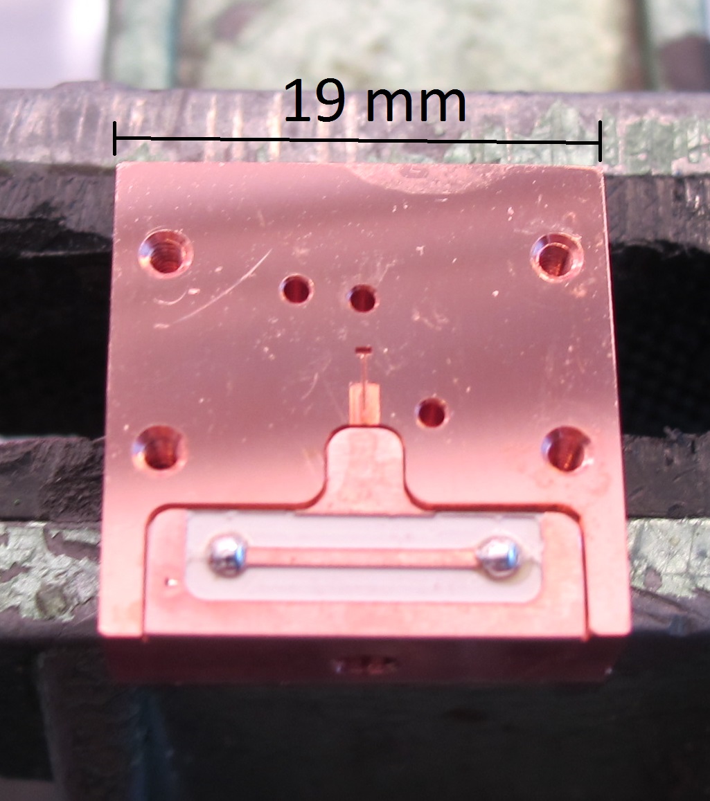
The detector design is an adaption of the lumped-element KID (LEKID) design. The signal is coupled via a high performance smooth-walled spline profile feedhorn to a waveguide and superconducting Niobium probe antenna. The RF circuitry is fabricated onto a device chip with a 9 µm Si membrane as substrate using the DRIE/MEMS fabrication technology developed for our HEB and SIS mixers. The RF signal is split into two coplanar waveguide (CPW) absorber lines with a 40 nm thick aluminum centerline as the absorbing part and Niobium ground planes. The CPW centerline forms the inductive section of a 2.5 GHz superconducting resonator, which is capacitively coupled to the readout line. Since the deposition of the centerline is a separate lithography step, the design also enables us to exchange the Al material and use the circuit as a testbed for kinetic inductance and loss measurements with other absorber materials. In addition to the LEKID, an identically coupled quarter-wave transmission line resonator will be compared to the detector design. Both circuits are designed with CST Microwave StudioTM for the high frequency parts of the circuit and Sonnet EMTM for the readout circuit.
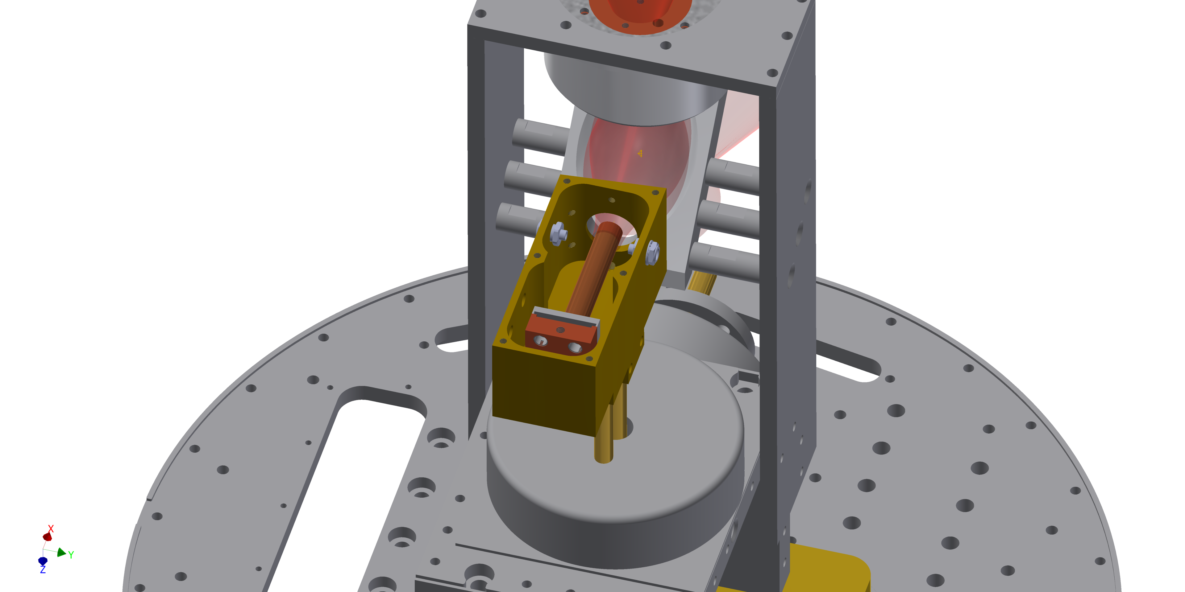
The MKID Devices need to be cooled to very low temperature. Typical operation temperatures of 100 mK can be achieved in our ADR cryostat.